-
Techcomp alkanes Ferroelectric fluoroalkane Organic CarbonNanotube Optoelectonics Styrene organic_polymer Polyvinylidene FloppyDisk DataStorage Celebration multi_layer Conduct MoS2 Floppy SurfaceChange CuSubstrate PinpointPFM semifluorinated alkane Vortex BaTiO3 Yeditepe Pinpoint PFM Pipette conductive CNT Praseodymium PyroelectricDetector temp_control AdhesionEnergy Wang Sic LightEmission
Report image
If you found this image unacceptable, please let us know. We will review your report and take action if we determine this image is really unacceptable.
Atomic steps on GaP(Gallium Phosphide) layer on Si
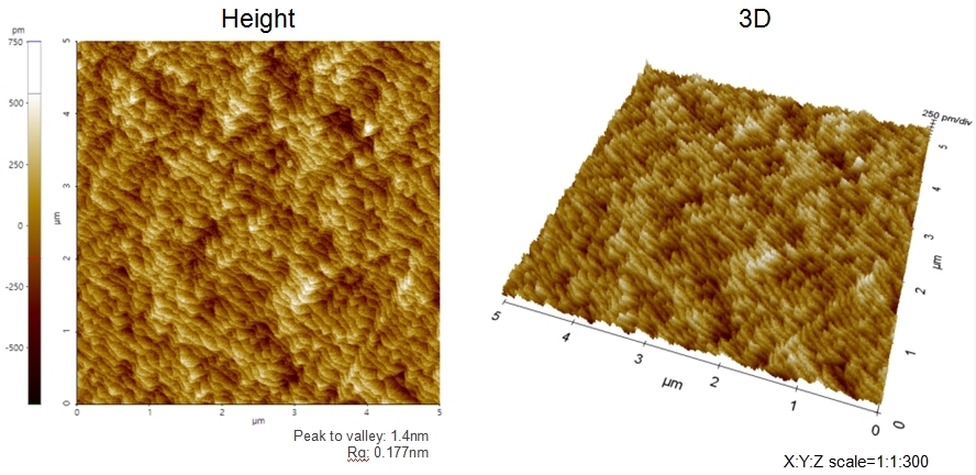
Scanning Conditions
- System: NX20
- Scan Mode: Non-contact
- Cantilever: PPP-NCHR (k=42N/m, f=300kHz)
- Scan Size: 5μm×5μm
- Scan Rate: 1Hz
- Pixel: 512×512