-
dielectric_trench self_assembly fluoroaalkane Polymer Array MfmAmplitude Cell Gallium AIN Molybdenum_disulfide Co/Cr/Pt Metal-organicComplex LeakageCurrent dichalcogenide Inorganic_Compound VortexCore organic_polymer fluoroalkane Cobalt chemical_compound BoronNitride AM_SKPM OpticalModulator HfO2 BTO Potential PinpointPFM Biofilm FailureAnalysis MechanicalProperties Chungnam_National_University SiliconCrystal HighResolution PetruPoni_Institute GalliumPhosphide
Report image
If you found this image unacceptable, please let us know. We will review your report and take action if we determine this image is really unacceptable.
Trench Etch Profile on Si Wafer
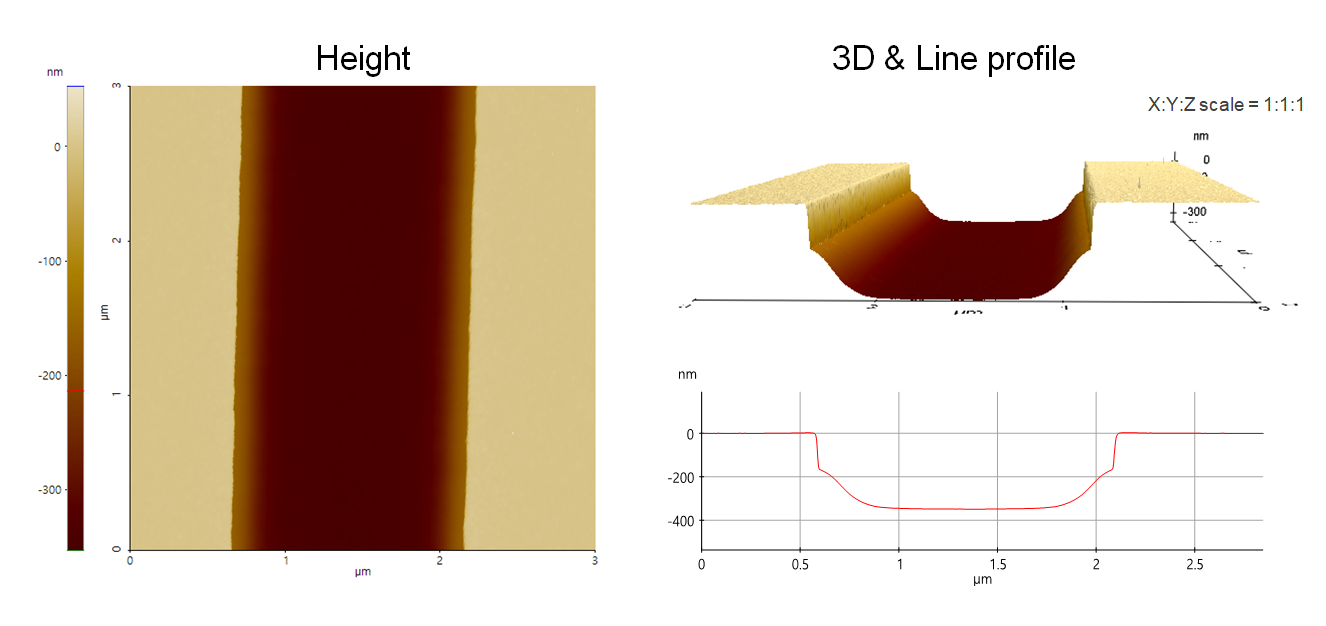
Top dielectric trench etch profile on Si wafer having tapered slope at the trench sidewall.
Scanning Conditions
- System: NX20
- Scan Mode: Non-contact
- Cantilever: AC160TS (k=26N/m, f=300kHz)
- Scan Size: 3μm×3μm
- Scan Rate: 0.21Hz
- Pixel: 1024 × 256
- Scan Mode: Non-contact
- Cantilever: AC160TS (k=26N/m, f=300kHz)
- Scan Size: 3μm×3μm
- Scan Rate: 0.21Hz
- Pixel: 1024 × 256