-
Change PpLdpe PolyimideFilm alkanes VerticalPFM DomainSwitching Ram ScratchMode Adhesion Semiconductor ElectroChemical Dr.JurekSadowski Barium_titanate SingleLayer EFMAmplitude OxideLayer Temasek_Lab StyreneBeads Ucl PolymerPatterns MagneticForce high_resolution Anneal Aggregated_molecules ForceMapping Alkane PUR 2-vinylpyridine mechanical_property BFO Ito graphene_hybrid FloppyDisk PtfeFilter Current
Report image
If you found this image unacceptable, please let us know. We will review your report and take action if we determine this image is really unacceptable.
MoS2 Layers on SiO2
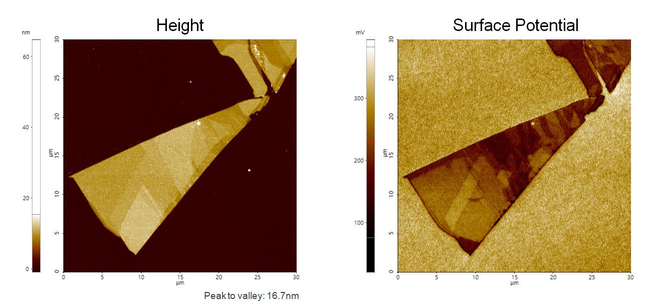
A few layers of MoS2 on SiO2
Scanning Conditions
- System: NX10
- Scan Mode: AM-KPFM
- Cantilever: NSC36Cr-Au B (k=2N/m, f=130kHz)
- Scan Size: 30μm×30μm
- Scan Rate: 0.3Hz
- Pixel Size: 512 × 256
- Scan Mode: AM-KPFM
- Cantilever: NSC36Cr-Au B (k=2N/m, f=130kHz)
- Scan Size: 30μm×30μm
- Scan Rate: 0.3Hz
- Pixel Size: 512 × 256