-
SurfaceOxidation conductive epitaxy ForceVolumeMapping Lateral IcelandSpar Techcomp dichalcogenide IMT_Bucharest Perovskite Chemical Vapor Deposition Semiconductor Forevision Corrosion Boron Aluminum CrAu PhaseImaging silicon_carbide Solar AM_KPFM fluorocarbon Film PVAP3HT SKKU StyreneBeads Leakage light_emission LateralPFM Titanate DeoxyribonucleicAcid optoelectronics neodymium_magnets HACrystal LightEmission
Report image
If you found this image unacceptable, please let us know. We will review your report and take action if we determine this image is really unacceptable.
Christmas Ball Lithography on Si
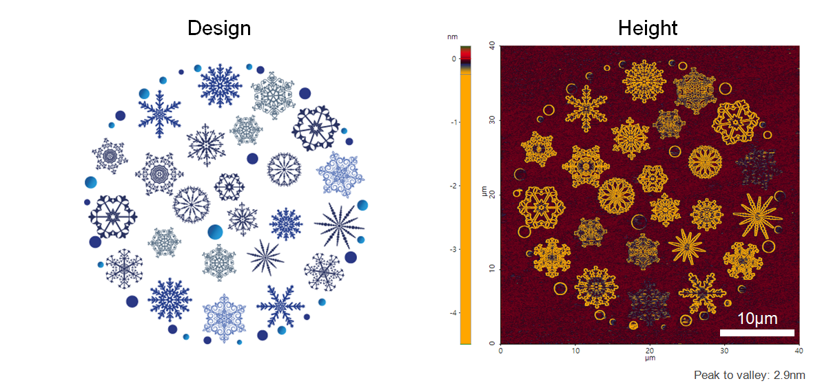
Create oxidation layers on bare Si surface using bias mode of lithography.
Scanning Conditions
- System: NX10
- Scan Mode: Lithography
- Cantilever: AD-40-SS (k=40N/m, f=200kHz)
- Scan Size: 40μm×40μm
- Scan Rate: 0.5Hz
- Pixel Size: 1024 × 1024
- Tip Bias: -10V for patterened area
- Scan Mode: Lithography
- Cantilever: AD-40-SS (k=40N/m, f=200kHz)
- Scan Size: 40μm×40μm
- Scan Rate: 0.5Hz
- Pixel Size: 1024 × 1024
- Tip Bias: -10V for patterened area