-
HfO2 Inorganic GaAs Piezoresponse AtomicSteps Regensburg BTO Aggregated_molecules Layer strontiu_titanate BariumTitanate HiVacuum GlassTemperature OpticalWaveguides PUR Defects Solution Typhimurium PolyvinylAcetate CHRYSALIS_INC CalciumHydroxyapatite NtuEee Modulus Carbon Laser 2d_materials Treatment Conducting TCS TyphimuriumBiofilm ThinFilm Fiber LiftMode dielectric trench Ni-FeAlloy
Report image
If you found this image unacceptable, please let us know. We will review your report and take action if we determine this image is really unacceptable.
Monolayer Graphene on PDMS Surface
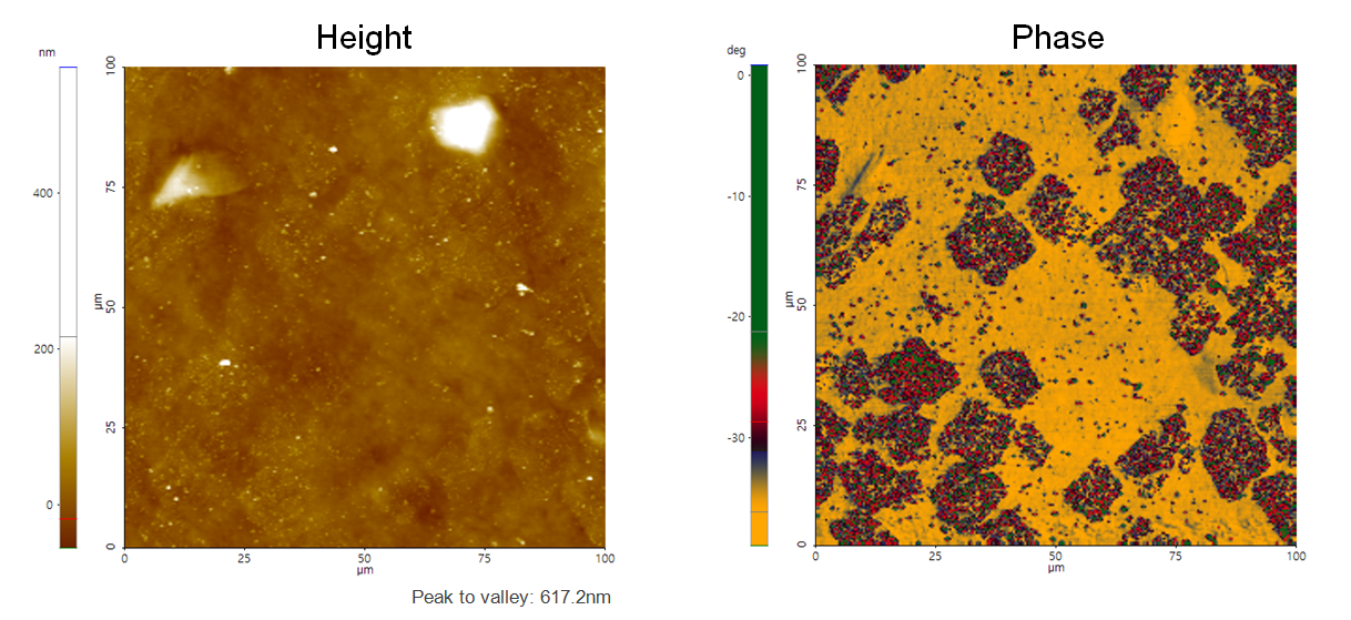
Monolayer Graphene grown on Cu foil using CVD process is transferred on to PDMS substrate.
Scanning Conditions
- System: NX20
- Scan Mode: Tapping
- Cantilever: Access-NC (k=113N/m, f=330kHz)
- Scan Size: 100μm×100μm
- Scan Rate: 0.6Hz
- Pixel Size: 256 × 256
- Scan Mode: Tapping
- Cantilever: Access-NC (k=113N/m, f=330kHz)
- Scan Size: 100μm×100μm
- Scan Rate: 0.6Hz
- Pixel Size: 256 × 256