-
SiliconOxide Aluminium_Oxide PolymerPatterns ito_film InorganicCompound Fluoride MagneticForce Pinpoint HBN TiO2 multi_layer 2dMaterials Conducting ReflexLens LateralForce Plug Yeditepe_University Jason Composite STM Copper KevlarFiber Aggregated_molecules Metal-organicComplex AtomicLayer AM_SKPM Piezoelectric Topography Ferroelectric CP-AFM Yttria_stabilized_Zirconia Anneal SRAM dielectric_trench oxide_layer
Report image
If you found this image unacceptable, please let us know. We will review your report and take action if we determine this image is really unacceptable.
Hard defect repair of photomask
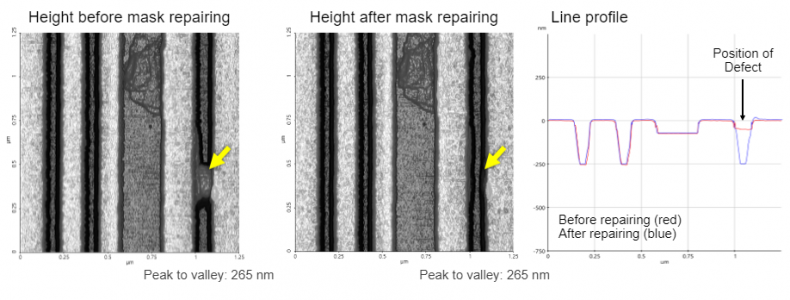
Scanning Conditions
- System : NX-Mask
- Scan Mode: Non-contact for imaging Sweep for repairing
- Scan Rate : 0.3 Hz
- Scan Size : 1.25μm×1.25μm
- Pixel Size : 256×256
- Cantilever : OMCL-AC160TS for imaging, AD-40 AS for repairing (k=42N/m, f=330kHz)