-
ScanningSpreadingResistanceMicroscopy Heating Ucl Semiconductor Dr.JurekSadowski contact Patterns fe_nd_b Perovskite domain_switching Tungsten_disulfide plastic SoftSample MESA structure hard_disk Lift AEAPDES aluminum_nitride Biofilm MonoLayer fluoroaalkane Piezo IRDetector Sapphire STO WPlug CastIron NUS_Physics heterojunctions Nanopattern HexagonalBN Zhi Sic Tape Chrome
Report image
If you found this image unacceptable, please let us know. We will review your report and take action if we determine this image is really unacceptable.
Strainded MoS₂ on Si
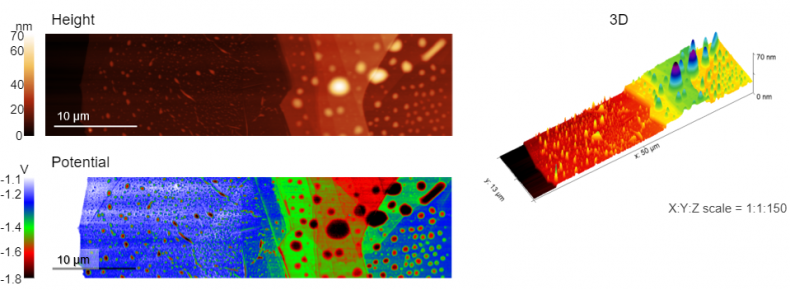
Scanning Conditions
- System : FX40
- Scan Mode: Sideband KPFM
- Scan Rate : 0.15Hz
- Scan Size : 50μm×13μm
- Pixel Size : 2048×1024
- Cantilever : ElectricMulti75-G (k=3N/m, f=75kHz)