-
Conductance Mfm OpticalElement ThermalDetectors Sidewall AdhesionForce Modulus pinpoint mode Hair Water Polydimethylsiloxane Granada University_of_Regensburg KelvinProbeForceMicroscopy Boron plastic light_emission Step Croatia Typhimurium Change conductive Blend LogAmplifier AtomicSteps SurfaceChange 2-vinylpyridine AM_SKPM AAO Steps cooling Ferrite self-assembly IRDetector PinpointPFM
Report image
If you found this image unacceptable, please let us know. We will review your report and take action if we determine this image is really unacceptable.
Atomic steps on GaP(Gallium Phosphide) layer on Si
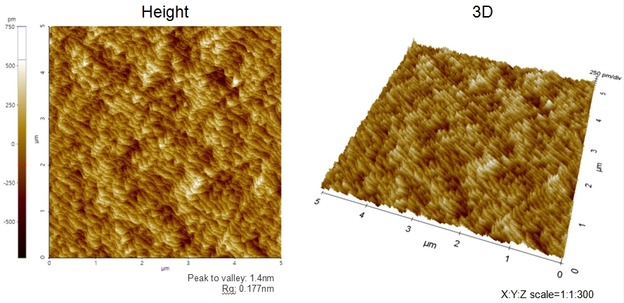
Scanning Conditions
- System: NX20
- Scan Mode: Non-contact
- Cantilever: PPP-NCHR (k=42N/m, f=300kHz)
- Scan Size: 5μm×5μm
- Scan Rate: 1Hz
- Pixel: 512×512