-
TipBiasMode atomic_layer Indent FailureAnlaysis Polydimethylsiloxane CVD ChemicalCompound RedBloodCell LeakageCurrent ImideMonomer ScanningKelvinProbeMicroscopy CuSubstrate SolarCell CuFoil dichalcogenide Wonseok Barium_titanate kelvin probe force microscopy Sio2 PANI FM_KPFM #Materials ShenYang Fe_film IIT-chennai Electrode INSPParis Indium_tin_oxide Calcium UTEM PinpointNanomechanicalMode Writing AEAPDES StrontiumTitanate LiBattery
Report image
If you found this image unacceptable, please let us know. We will review your report and take action if we determine this image is really unacceptable.
ITO Film Sputter Deposited onto Silicon
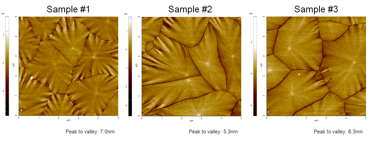
ITO-film, which was sputter deposited onto silicon. The grain size of those samples was influenced by changing the process settings in the Cluterline RAD sputter deposition system, one of the deposition tool platforms manufactured by Evatec.
Scanning Conditions
- System: NX10
- Scan Mode: Non-contact
- Cantilever: PPP-EFM (k=2.8N/m, f=75kHz)
- Scan Size: 5μm×5μm
- Scan Rate: 0.1Hz
- Pixel Size: 256 × 256
- Scan Mode: Non-contact
- Cantilever: PPP-EFM (k=2.8N/m, f=75kHz)
- Scan Size: 5μm×5μm
- Scan Rate: 0.1Hz
- Pixel Size: 256 × 256