-
Copper PolycrystallineFerroelectricBCZT Wonseok DeoxyribonucleicAcid LMF VortexCore ForceVolumeMapping Microchannel MonoLayer Bismuth Chloroform Sio2 mechanical property Conductance fifber LogAmplifier atomic_steps Vortex China AtomicLayer PS_PVAC strontiu_titanate amplitude_modulation Hydroxyapatite AEAPDES IISCBangalore Friction atomic_layer Polytetrafluoroethylene 2dMaterials Hole NeodymiumMagnets Polymer EFM Composition
Report image
If you found this image unacceptable, please let us know. We will review your report and take action if we determine this image is really unacceptable.
Trench Etch Profile on Si Wafer
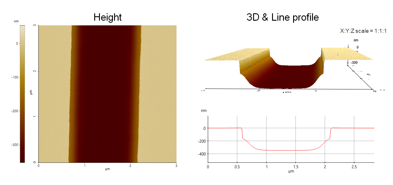
Top dielectric trench etch profile on Si wafer having tapered slope at the trench sidewall.
Scanning Conditions
- System: NX20
- Scan Mode: Non-contact
- Cantilever: AC160TS (k=26N/m, f=300kHz)
- Scan Size: 3μm×3μm
- Scan Rate: 0.21Hz
- Pixel: 1024 × 256
- Scan Mode: Non-contact
- Cantilever: AC160TS (k=26N/m, f=300kHz)
- Scan Size: 3μm×3μm
- Scan Rate: 0.21Hz
- Pixel: 1024 × 256