-
Sadowski Polyaniline Hexatriacontane Molybdenum AtomicLayer Wonseok GaAs BCZT MechanicalProperties Bacterium EvatecAG Phthalocyanine self-assembly ContactMode 3-hexylthiophene InLiquid CVD chemical_compound SurfaceOxidation PvdfBead MoirePattern ImideMonomer LaAlO3 2d_materials LiIonBattery Nanopattern BariumTitanate mechanical property Jason 2dMaterials ElectrostaticForceMicroscopy temp ULCA HighAcpectRatio silicon_carbide
Report image
If you found this image unacceptable, please let us know. We will review your report and take action if we determine this image is really unacceptable.
Patterned Sapphire Substrate (PSS)
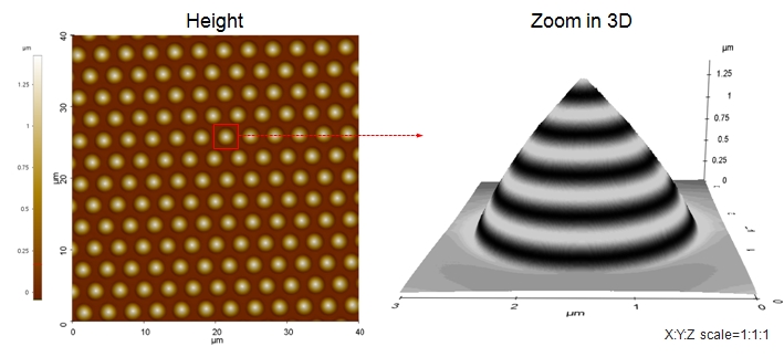
Scanning Conditions
- System: NX10
- Scan Mode: Non-contact
- Cantilever: AR5T-NCHR
- Scan Size: 40μm×40μm, 3μm×3μm
- Scan Rate: 0.3Hz, 1Hz
- Pixel: 256 × 256
- Scan Mode: Non-contact
- Cantilever: AR5T-NCHR
- Scan Size: 40μm×40μm, 3μm×3μm
- Scan Rate: 0.3Hz, 1Hz
- Pixel: 256 × 256