-
Nanotechnology Optoelectronic ring shape Chemical Vapor Deposition Molybdenum_disulfide Topography molecular_beam Oxidation PatternedSapphireSubstrat Kevlar non_contact PiezoelectricForceMicroscopy FM-KPFM bias_mode Lateral_Force_Microscopy ThermalConductivity Celebration FM_SKPM Cross-section KevlarFiber OpticalElement PvdfFilm HexagonalBN Pinpoint PFM Platinum Implant Grain Writing Lateral SRAM Austenite University_of_Regensburg CuFoil CeNSE_IISc FAFailureAnlaysis
Report image
If you found this image unacceptable, please let us know. We will review your report and take action if we determine this image is really unacceptable.
Self-assembly of Semi-fluorinated Alkanes
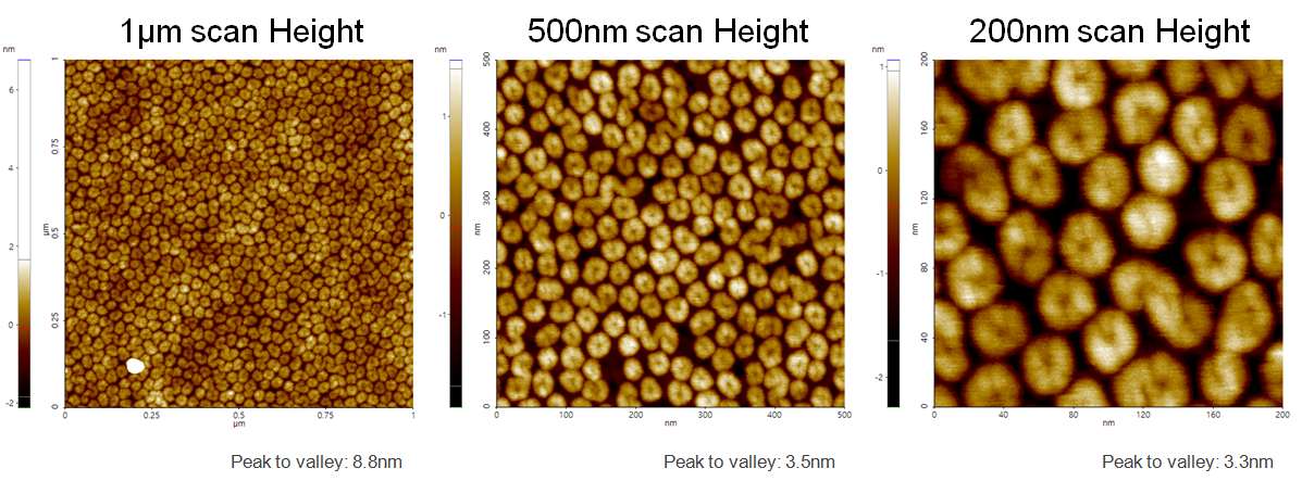
Domains formed by the self-assembly of semi-fluorinated alkanes deposited as a monolayer on the surface of the water. The monolayer was compressed before being transferred onto a silicon substrate. Each domain includes about 4000 molecules. The domains were easily detached from the substrate with tapping mode because the molecules were very loosely attached to the substrate. Only Non-contact mode could achieve this result.
Scanning Conditions
- System: NX10
- Scan Mode: Non-contact
- Cantilever: PPP-FMR (k=2.8N/m, f=75kHz)
- Scan Size: 1μm×1μm, 0.5μm×0.5μm, 0.2μm×0.2μm
- Scan Rate: 2Hz
- Pixel Size: 500 × 500
- Scan Mode: Non-contact
- Cantilever: PPP-FMR (k=2.8N/m, f=75kHz)
- Scan Size: 1μm×1μm, 0.5μm×0.5μm, 0.2μm×0.2μm
- Scan Rate: 2Hz
- Pixel Size: 500 × 500