-
SPMLabs Singapore alkanes ForceMapping HardDiskMedia MonoLayer Magnets FailureAnlaysis HiVacuum plastic Ni-FeAlloy margarine Gallium SThM Ceramic cannabinoid Pores Mosfet HydroGel Korea CalciumHydroxyapatite AM_KPFM KelvinProbeForceMicroscopy C60H122 Hafnia Non-ContactMode exfoliate Semiconductor Chloroform BariumTitanate MagneticForceMicroscopy AEAPDES TungstenDeposition Platinum Graphene
Report image
If you found this image unacceptable, please let us know. We will review your report and take action if we determine this image is really unacceptable.
Trench Etch Profile on Si Wafer
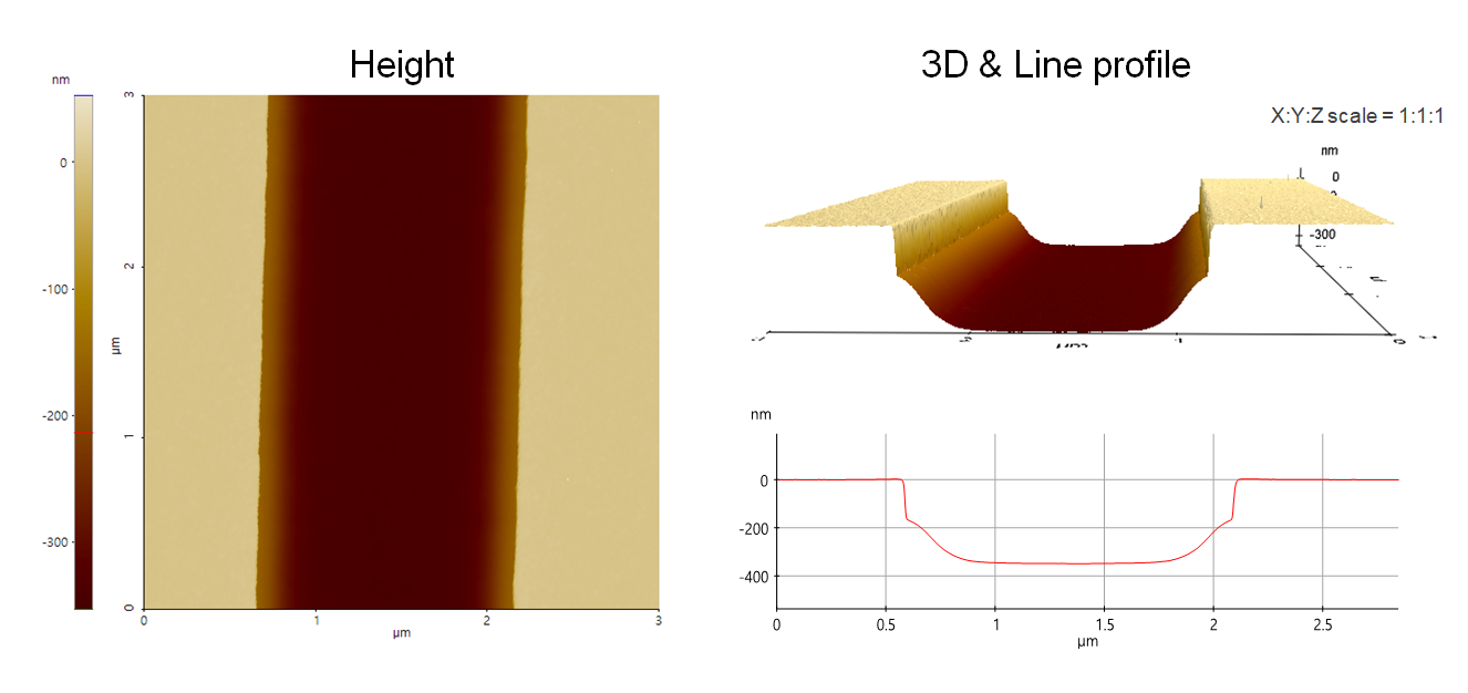
Top dielectric trench etch profile on Si wafer having tapered slope at the trench sidewall.
Scanning Conditions
- System: NX20
- Scan Mode: Non-contact
- Cantilever: AC160TS (k=26N/m, f=300kHz)
- Scan Size: 3μm×3μm
- Scan Rate: 0.21Hz
- Pixel: 1024 × 256
- Scan Mode: Non-contact
- Cantilever: AC160TS (k=26N/m, f=300kHz)
- Scan Size: 3μm×3μm
- Scan Rate: 0.21Hz
- Pixel: 1024 × 256