-
CastIron Vacuum Resistance MechanicalProperty ScanningTunnelingMicroscopy StrontiuTitanate pinpoint mode fluoroalkane CeramicCapacitor Mechanical&nanotechnology Global_Comm HighAcpectRatio HanyangUniv BreastCancerCell Device CHRYSALIS_INC LeakageCurrent cannabinoid Tin disulfide Battery Foil VortexCore Ptfe SurfaceChange Fiber Organic temp StyreneBeads Morphology Tapping pulsed_laser_deposition NeodymiumMagnets Edwin Temasek_Lab layers
Report image
If you found this image unacceptable, please let us know. We will review your report and take action if we determine this image is really unacceptable.
Taegeuk Mark Lithography on PZT
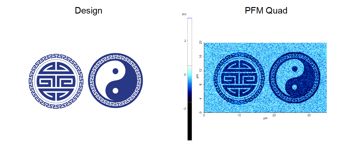
Re-arranged the domain pole direction on PZT surface using bias mode of lithography.
Scanning Conditions
- System: NX10
- Scan Mode: Lithography
- Cantilever: PPP-ContScPt (k=0.2N/m, f=25kHz)
- Scan Size: 35μm×20μm
- Scan Rate: 0.5Hz
- Pixel Size: 1024 × 1024
- Tip Bias: 10V for patterned area
- Scan Mode: Lithography
- Cantilever: PPP-ContScPt (k=0.2N/m, f=25kHz)
- Scan Size: 35μm×20μm
- Scan Rate: 0.5Hz
- Pixel Size: 1024 × 1024
- Tip Bias: 10V for patterned area