-
chemical_compound Fujian Phenanthrene Reading EPFL Cancer HBN Deposition Croatia Force-distance C36H74 Yeditepe_University Mechinical CeNSE_IISc NeodymiumMagnets Galfenol AtomicSteps Tin disulfide ReflexLens dielectric_trench Permalloy contact SiWafer Polymer IISCBangalore TipBiasMode Polarization Magnetic Force Microscopy Korea cannabis YttriaStabilizedZirconia Laser Semiconductor Piezo GranadaUniv
Report image
If you found this image unacceptable, please let us know. We will review your report and take action if we determine this image is really unacceptable.
GaN epi wafer
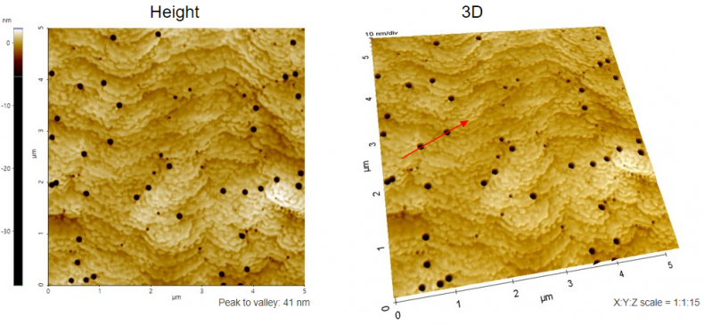
Scanning Conditions
- System : NX-Wafer
- Scan Mode: Non-contact
- Scan Rate : 0.7 Hz
- Scan Size : 5μm×5μm
- Pixel Size : 512×512
- Cantilever : PPP-NCHR (k=42N/m, f=330kHz)