-
Leakage Vacuum Yeditepe_University aluminum_nitride CNT TPU Polymer BreastCancerCell Nickel C36H74 exfoliate FloppyDisk LightEmission Magnetic Force Microscopy AM_KPFM Film ScanningThermalMicroscopy Polarization Barium_titanate Galfenol medical HanyangUniv STM bias_mode Polyvinylidene_fluoride silicon_oxide hard_disk_media SiliconCrystal Array Tungsten_disulfide Silicon PVAP3HT heterojunctions Singapore Co/Cr/Pt
Report image
If you found this image unacceptable, please let us know. We will review your report and take action if we determine this image is really unacceptable.
Copper film
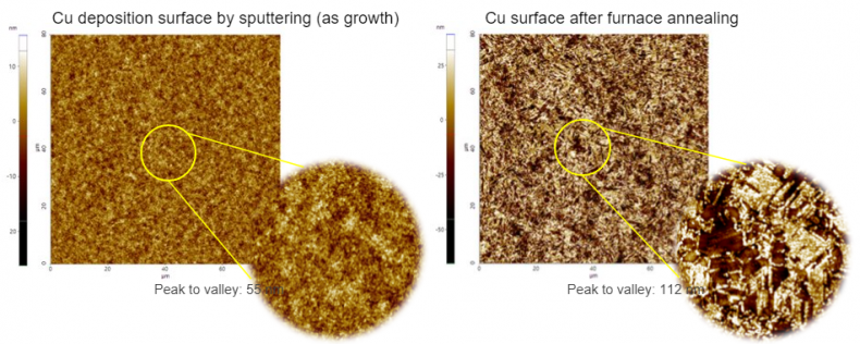
Scanning Conditions
- System : NX-Wafer
- Scan Mode: Non-contact
- Scan Rate : All 1Hz
- Scan Size : All 512μm×256μm
- Pixel Size : 512×512
- Cantilever : OMCL-AC160TS (k=26N/m, f=300kHz)