-
dielectric_trench WPlug SRAM Epoxy Polytetrafluoroethylene Pyroelectric SoftSample PANI Steps Non-ContactMode cannabis Collagen nanomechanical Gallium_Arsenide PhthalocyaninePraseodymium #Materials Optical PetruPoni_Institute HDD ScanningThermalMicroscopy FAPbI3 Chemical_Vapor_Deposition FFM Chemical Vapor Deposition Piranha Composite sputter vertical_PFM Alloy LiIonBattery UnivMaryland INSPParis IMT_Bucharest HfO2 PVAC
Report image
If you found this image unacceptable, please let us know. We will review your report and take action if we determine this image is really unacceptable.
2L-MoS₂ (2/3)
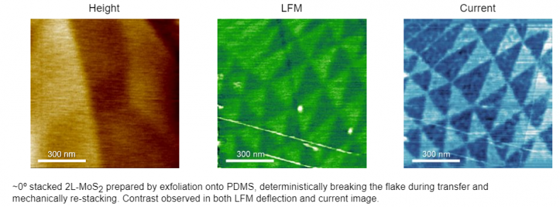
Scanning Conditions
- System : FX40
- Sample bias: 0.5 V
- Scan Mode: C-AFM, LFM
- Scan Rate : 12 Hz
- Scan Size : 1μm×1μm
- Pixel Size : 512×512
- Cantilever : ElectricMulti75-G (k=3N/m, f=75kHz)