-
FAPbI3 Silicon Laser electrospinning Tin disulfide atomic_layer FFM Non-ContactMode dielectric_trench Adhesion Roughness Optoelectonics SKKU PolycrystallineFerroelectricBCZT CeNSE_IISc Liquid PFM #Materials Forevision frequency_modulation FM_SKPM neodymium_magnets Morphology Polytetrafluoroethylene C60H122 Polyaniline tip_bias_mode Christmas UTEM Foil OpticalWaveguide TempControl OrganicCompound ForceVolumeMapping HydroGel
Report image
If you found this image unacceptable, please let us know. We will review your report and take action if we determine this image is really unacceptable.
Polymer patterns on Si (1/2)
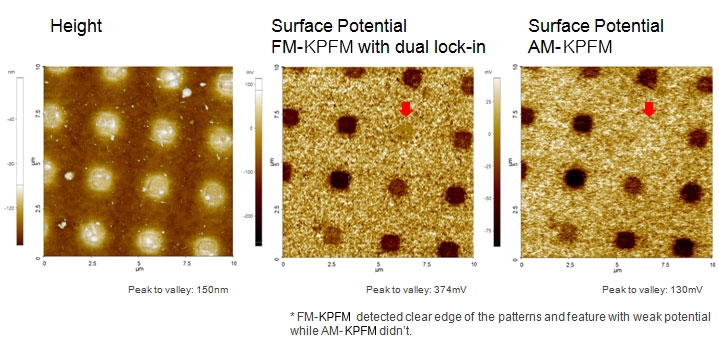
Scanning Conditions
- System: NX10
- Scan Mode: KPFM
- Cantilever: NSC36Cr-Au (k=1N/m, f=90kHz)
- Scan Size: 10μm×10μm
- Scan Rate: 0.2Hz
- Pixel: 512×256