-
Electronics Lattice Sadowski ElectrostaticForceMicroscopy LiNbO3 Fluoride LiftHeight Heating FuelCell Morphology HBN TemperatureControllerAFM mechanical_property Beads Varistor PFM Adhesion AtomicSteps HfO2 Growth Ptfe Ferrite TempControl Wang ScanningTunnelingMicroscopy StrontiumTitanate SiWafer contact Device LightEmiting Collagen MetalCompound lift_mode Conduct Sperm
Report image
If you found this image unacceptable, please let us know. We will review your report and take action if we determine this image is really unacceptable.
Taegeuk Mark Lithography on PZT
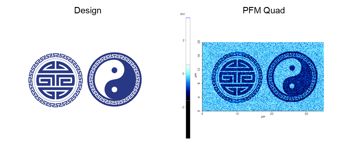
Re-arranged the domain pole direction on PZT surface using bias mode of lithography.
Scanning Conditions
- System: NX10
- Scan Mode: Lithography
- Cantilever: PPP-ContScPt (k=0.2N/m, f=25kHz)
- Scan Size: 35μm×20μm
- Scan Rate: 0.5Hz
- Pixel Size: 1024 × 1024
- Tip Bias: 10V for patterned area
- Scan Mode: Lithography
- Cantilever: PPP-ContScPt (k=0.2N/m, f=25kHz)
- Scan Size: 35μm×20μm
- Scan Rate: 0.5Hz
- Pixel Size: 1024 × 1024
- Tip Bias: 10V for patterned area