-
GaN Hole PFM ScanningIon-ConductanceMicroscopy Growth VinylAlcohol Gallium_Arsenide strontiu_titanate Bio PolyimideFilm AAO LightEmiting Current Glass LiftHeight CntFilm Wafer Collagen HighAcpectRatio Multiferroic_materials Adhesive cannabis Hair Temperature Sphere BaTiO3 NUS_NNI_Nanocore Oxide BismuthVanadate Corrosion Bacteria Composition Crystal hetero_structure OpticalElement
Report image
If you found this image unacceptable, please let us know. We will review your report and take action if we determine this image is really unacceptable.
Monolayer Graphene on PDMS Surface
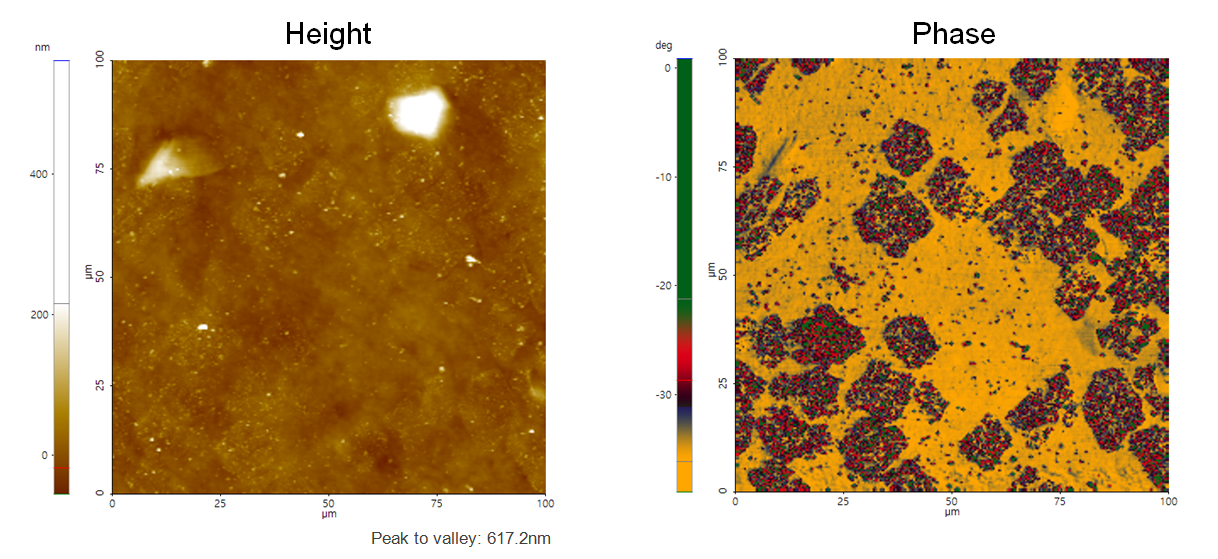
Monolayer Graphene grown on Cu foil using CVD process is transferred on to PDMS substrate.
Scanning Conditions
- System: NX20
- Scan Mode: Tapping
- Cantilever: Access-NC (k=113N/m, f=330kHz)
- Scan Size: 100μm×100μm
- Scan Rate: 0.6Hz
- Pixel Size: 256 × 256
- Scan Mode: Tapping
- Cantilever: Access-NC (k=113N/m, f=330kHz)
- Scan Size: 100μm×100μm
- Scan Rate: 0.6Hz
- Pixel Size: 256 × 256