-
Yttria_stabilized_Zirconia atomic_steps Adhesive IMT_Bucharest Polyvinylidene_fluoride heterojunctions Non-ContactMode F14H20 Neodymium C60H122 ContactMode Composite atomic_layer Pattern MetalCompound tip_bias_mode SAM Barium_titanate Edwin FrictionalForce Display ThermalProperties Litho PvdfFilm SelfAssembly Ecoli Ni81Fe19 Ceramic LaAlO3 Wang mechanical_property BFO Hafnium_dioxide Polyimide conductive
Report image
If you found this image unacceptable, please let us know. We will review your report and take action if we determine this image is really unacceptable.
BN thin film on Si
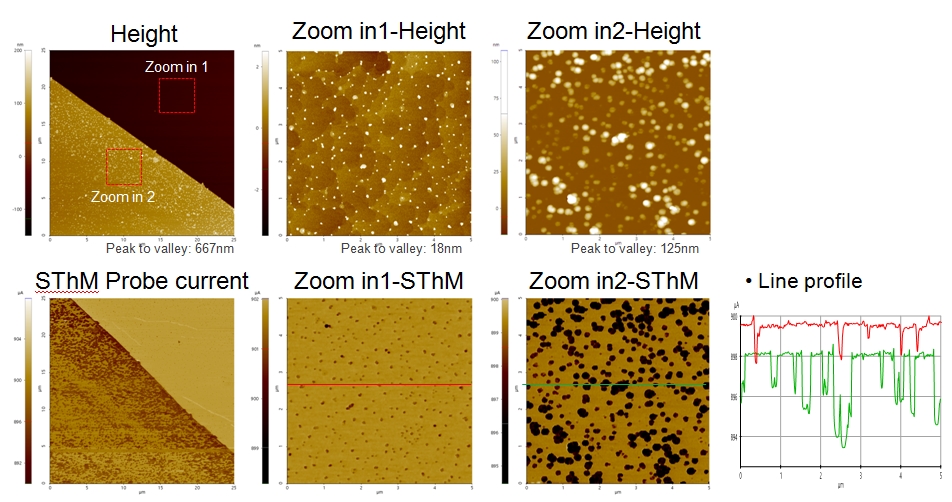
Scanning Conditions
- System: NX10
- Scan Mode:SThM
- Cantilever: Nanothermal probe
- Scan Size: 25μm×25μm, 5μm×5μm
- Scan Rate:0.3Hz, 0.5Hz
- Pixel: 256×256, 256×256
- Scan Mode:SThM
- Cantilever: Nanothermal probe
- Scan Size: 25μm×25μm, 5μm×5μm
- Scan Rate:0.3Hz, 0.5Hz
- Pixel: 256×256, 256×256