-
MultiLayerCeramicCapacitor HardDisk biocompatible layers UnivMaryland self_healing TyphimuriumBiofilm NtuEee AM-KPFM silicon_carbide SiliconCrystal NUS UnivCollegeLondon contact Fet CHRYSALIS_INC 3-hexylthiophene Switching Nanofiber UTEM TPU InLiquid CNT StrontiumTitanate graphene_hybrid oxide_layer Polytetrafluoroethylene LightEmiting Titanate LifeScience Gold Ca10(PO4)6(OH)2 semifluorinated_alkane Edwin SrO
Report image
If you found this image unacceptable, please let us know. We will review your report and take action if we determine this image is really unacceptable.
MoS2 Layers on SiO2
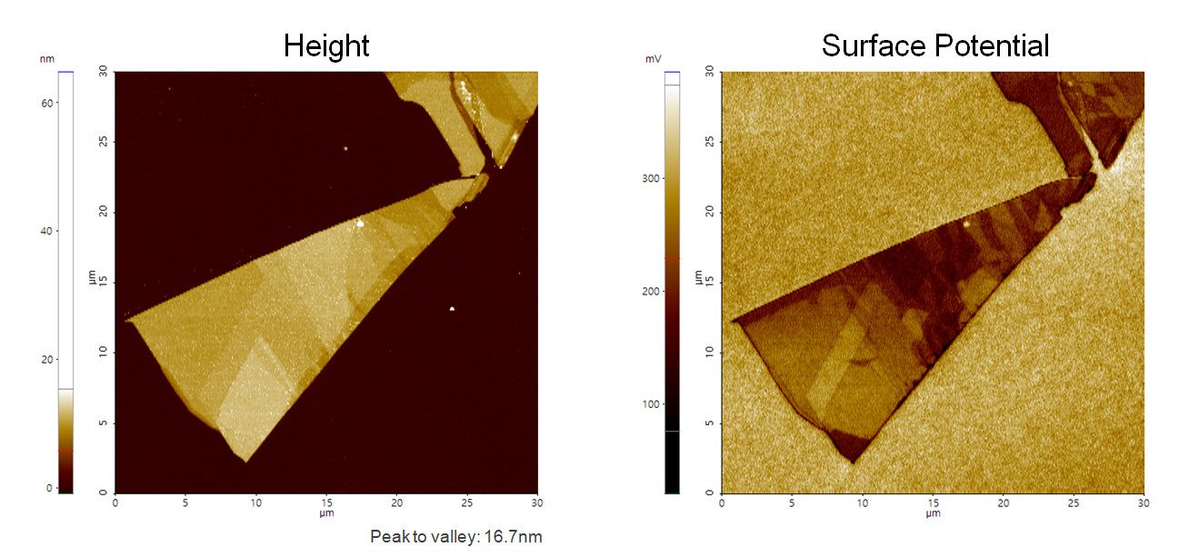
A few layers of MoS2 on SiO2
Scanning Conditions
- System: NX10
- Scan Mode: AM-KPFM
- Cantilever: NSC36Cr-Au B (k=2N/m, f=130kHz)
- Scan Size: 30μm×30μm
- Scan Rate: 0.3Hz
- Pixel Size: 512 × 256
- Scan Mode: AM-KPFM
- Cantilever: NSC36Cr-Au B (k=2N/m, f=130kHz)
- Scan Size: 30μm×30μm
- Scan Rate: 0.3Hz
- Pixel Size: 512 × 256