-
plastics PVA Tungsten neodymium_magnets Boundary FM_KPFM Self-assembledMonolayer Spain Celebration Polarization SFAs Wildtype StrontiuTitanate BiVO4 rubber CalciumHydroxide Scanning_Thermal_Microscopy lift_mode Litho FrictionForce CalciumHydroxyapatite doped Anneal Layer FastScan AEAPDES Ceramic single_layer #EC graphene_hybrid SKKU Granada Chemical Vapor Deposition TyphimuriumBiofilm Tin sulfide
Report image
If you found this image unacceptable, please let us know. We will review your report and take action if we determine this image is really unacceptable.
Monolayer Graphene on PDMS Surface
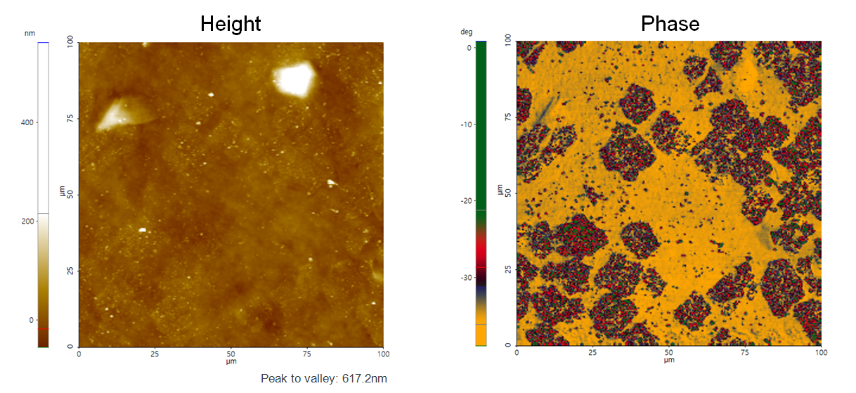
Monolayer Graphene grown on Cu foil using CVD process is transferred on to PDMS substrate.
Scanning Conditions
- System: NX20
- Scan Mode: Tapping
- Cantilever: Access-NC (k=113N/m, f=330kHz)
- Scan Size: 100μm×100μm
- Scan Rate: 0.6Hz
- Pixel Size: 256 × 256
- Scan Mode: Tapping
- Cantilever: Access-NC (k=113N/m, f=330kHz)
- Scan Size: 100μm×100μm
- Scan Rate: 0.6Hz
- Pixel Size: 256 × 256