-
Lateral_Force_Microscopy Zhi CrossSection epitaxy TemperatureControl domain_switching Tapping UnivOfMaryland CBD gallium_nitride Anneal small_scan MBE LiftMode HumanHair Calcium Step SFAs bias_mode medical LiquidCell Ceramic Chungnam_National_University SrO Pore Electronics LifeScience Platinum INSP Polyethylene Magnets NeodymiumMagnets China vertical_PFM Insulator
Report image
If you found this image unacceptable, please let us know. We will review your report and take action if we determine this image is really unacceptable.
Photoresist pattern (post-development process)
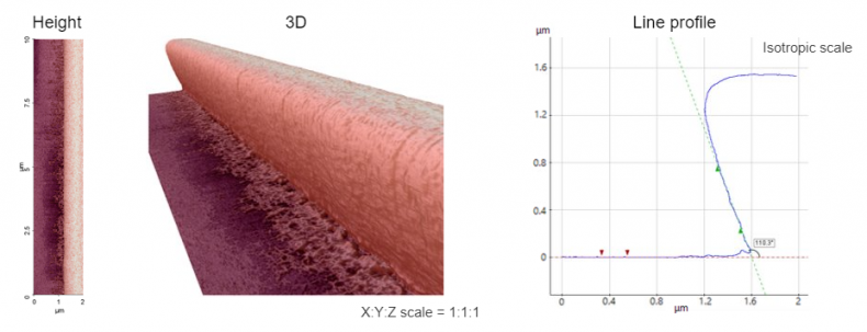
Scanning Conditions
- System : NX-3DM
- Scan Mode: Non-contact
- Scan Rate : 0.1 Hz
- Scan Size : 2μm×10μm
- Pixel Size : 512×2048
- Cantilever : EBD-R2-NCLR (k=45N/m, f=190kHz)