-
Hexylthiophene TemperatureControl Scanning_Thermal_Microscopy LaAlO3 Lift LiBattery BloodCell Blood Current TyphimuriumBiofilm IISCBangalore molecular_self_assembly Vinylpyridine TappingMode Zagreb Piezo Polypropylene biocompatible kelvin probe force microscopy Device OrganicCompound PetruPoni Topography HydroGel India HDD Co/Cr/Pt non_contact light_emission cannabis SiliconCrystal Composite Spain temp Inorganic
Report image
If you found this image unacceptable, please let us know. We will review your report and take action if we determine this image is really unacceptable.
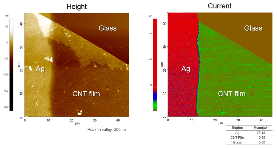
CNT Film
Scanning Conditions
- System: NX10
- Scan Mode: CP-AFM
- Cantilever: CDT-Contr (k=0.5N/m, f=20kHz)
- Scan Size: 45μm×45μm
- Scan Rate: 0.5Hz
- Pixel: 512×512
- Sample Bias: +0.3V
- Scan Mode: CP-AFM
- Cantilever: CDT-Contr (k=0.5N/m, f=20kHz)
- Scan Size: 45μm×45μm
- Scan Rate: 0.5Hz
- Pixel: 512×512
- Sample Bias: +0.3V