-
thermoplastic_elastomers Chromium ring shape Annealed NUSNNI AmplitudeModulation ForceDistanceSpectroscopy NtuEee Defects STO Memory Potential Terrace KevlarFiber Tungsten VinylAlcohol Temperature Led Chemical Vapor Deposition Anneal FAFailureAnlaysis Praseodymium GlassTemperature PrCurve Mosfet SiWafer BlockCopolymer Monisha Film Optic Indium_tin_oxide BoronNitride FFM Magnetostrictive CP-AFM
Report image
If you found this image unacceptable, please let us know. We will review your report and take action if we determine this image is really unacceptable.
Atomic steps on GaP(Gallium Phosphide) layer on Si
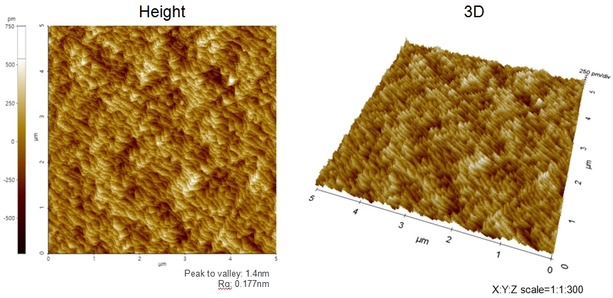
Scanning Conditions
- System: NX20
- Scan Mode: Non-contact
- Cantilever: PPP-NCHR (k=42N/m, f=300kHz)
- Scan Size: 5μm×5μm
- Scan Rate: 1Hz
- Pixel: 512×512