-
PvdfBead Electrode lift_mode Neodymium LightEmiting NtuEee Electical&Electronics EvatecAG Optic SolarCell optoelectronics HfO2 AtomicSteps MeltingPoint Molybdenum_disulfide Morphology nanobar Au111 Switching Solution Nickel Conductivity Fendb LiquidCrystal Defects Ananth dichalcogenide Pattern Zagreb CastIron Pore Co/Cr/Pt Pinpoint PFM HexagonalBoronNitride membrane
Report image
If you found this image unacceptable, please let us know. We will review your report and take action if we determine this image is really unacceptable.
Multi-layer necking device defect
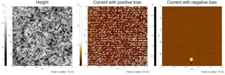
Scanning Conditions
- System : NX-Wafer
- Scan Mode: C-AFM
- Scan Rate : 2Hz
- Scan Size : 2μm×2μm
- Pixel Size : 512×256
- Cantilever : AD-2.8-AS (k=2.8N/m, f=75kHz)